IBM Shows Sub-1 Nanometer Chip Research, With Production Proof Still Missing
IBM unveiled a 0.7 nm nanostack chip technology with nearly 100 billion transistors, but the company has not announced a manufacturing partner, production date or customer design win.
IBM Pushes Chip Scaling Below One Nanometer
IBM has unveiled a sub-1 nanometer chip technology built around a three-dimensional nanostack transistor architecture, presenting the research as a way to extend semiconductor scaling as conventional designs approach atomic dimensions.
The company described the node as 0.7 nm, or 7 angstroms.
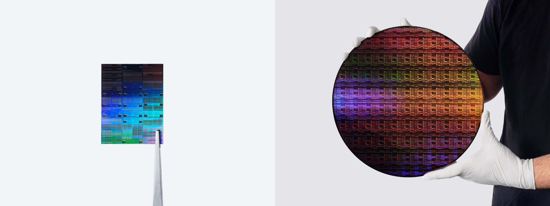
It said the research device reaches nearly 100 billion transistors on a fingernail-scale die, a density level IBM compared with the 2 nm chip it unveiled in 2021.
The announcement is important for AI compute because training and inference workloads keep pushing the industry toward denser and more energy-efficient logic.
IBM projected a performance gain of up to 50 percent, or a 70 percent energy-efficiency improvement, against its 2 nm node chips.
Those figures are research projections, not shipping product claims.
IBM also framed the advance as a response to the limits of traditional chip scaling.
The company said semiconductors are central to computing, appliances, communications devices, transportation systems and critical infrastructure, which makes any credible path to denser logic relevant beyond a single product line.
IBM did not announce a manufacturing partner, production date, foundry process transfer, first customer design or commercial chip family using the new architecture.
Nanostack Changes The Transistor Layout
IBM said nanostack is a three-dimensional, nanosheet-based design that vertically stacks and staggers transistors.
The design uses 3D sequential integration to increase transistor density and allows different material combinations within stacked layers.
The company said researchers had tested the architecture through CMOS integration work involving ultra-thin dielectric bonding, dual-channel engineering and functional inverter operation.
Those claims show that IBM is presenting the work as more than a drawing-board roadmap, while still keeping it in the research stage.
IBM also cited research presented at VLSI 2026 showing 40 percent scaling in SRAM.
That memory detail matters for advanced AI workloads because SRAM density and bandwidth shape how quickly chips can move data close to compute.
The design also gives IBM a materials argument.
By allowing different material combinations inside stacked layers, nanostack is meant to tune power efficiency and performance separately across parts of the transistor structure.
IBM did not say which foundry process or supply chain would carry that materials work into commercial manufacturing.
AI Compute Still Needs A Commercial Path
IBM framed the work as a decade-long scaling path for logic technology below the 1 nm node.
It also connected the architecture to generative AI, cloud infrastructure and electronic devices that require higher performance per watt.
Jay Gambetta, director of IBM Research and an IBM Fellow, said the nanostack architecture is meant to reinvent how chips are built for more power and energy efficiency.
The statement makes clear that IBM is positioning the work as a platform-level research advance rather than a single processor launch.
The timing also matters for customers planning AI infrastructure.
Better performance per watt can reduce pressure on data-center power budgets only if the technology reaches manufacturable chips with acceptable yield, cost and packaging support.
IBM's release does not provide those manufacturing economics.
The commercial burden remains outside the announcement.
IBM has technical validation, density targets and performance projections for sub-1 nm logic, but it has not named the factory, production schedule, chip customers or yield evidence needed to turn nanostack research into deployed AI compute.