Japan's deep-tech startup Flosfia offers next-gen power chips that allow EVs to travel farther
Kyoto University startup Flosfia is developing gallium oxide power semiconductors as an alternative to silicon for devices including electric vehicles. The company says gallium oxide delivers far lower power loss than silicon and silicon carbide, while its mist CVD process can bring production costs close to silicon. Flosfia says its devices have met industry reliability criteria and is preparing for mass production with a target of 1 million units per month.
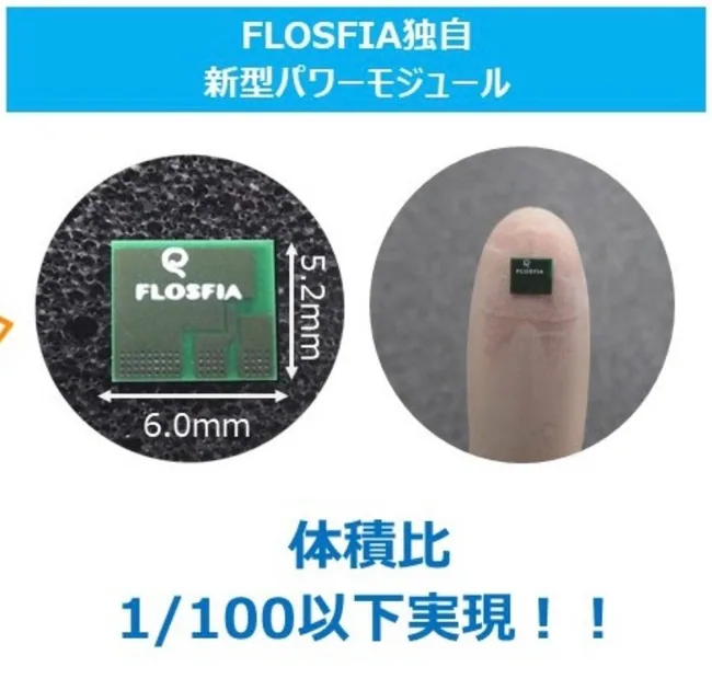
Japan's deep-tech startup Flosfia is developing next-generation power semiconductors based on gallium oxide, a material the company says can outperform traditional silicon in devices ranging from smartphones and PCs to electric vehicles and solar power equipment.
Founded in March 2011 as a startup from Kyoto University, Flosfia has a plant and development department near the university's Katsura campus.
The company is among the players working toward mass production of gallium oxide power semiconductors, which Japanese researchers see as having the potential to vastly exceed silicon performance.
Gallium oxide and lower power loss
Power semiconductors are designed to handle high currents and voltages while keeping power consumption low.
Silicon has long been the standard material, though silicon carbide and gallium nitride are also being adopted as next-generation options.
Flosfia says gallium oxide offers even higher performance.
The material has an extremely hard corundum crystal structure, similar to rubies and sapphires.
According to the company, its low power loss is 7,000 times better than silicon and 20 times better than silicon carbide.
Current president Toshimi Hitora, who joined Flosfia in 2012, shifted the company's earlier desalination filtration membrane technology business toward power semiconductors.
Hitora told J-Stories that gallium oxide power semiconductors can be produced at one-fifth to one-tenth the cost of silicon carbide and gallium nitride equivalents.
Mist CVD, partners and funding
Part of that cost position comes from a "mist CVD" method conceived at Kyoto University and then developed by Flosfia.
The process deposits a thin metal film at the atomic level, helping reduce the cost of semiconductors made from new materials to close to that of silicon.
Flosfia is working with companies, universities and research institutions on gallium oxide power semiconductor research and development.
Those involved include Novel Crystal Technology, a startup in Saitama Prefecture.
Investors include auto parts manufacturer Denso, industrial robot maker Yaskawa Electric and air-conditioning company Daikin Industries.
Reliability targets and patent portfolio
According to the company, its gallium oxide semiconductors have already met all industry criteria for reliability, with mass production the next step.
Flosfia hopes to reach output of 1 million units per month.
To date, the company has applied for around 700 patents and been granted more than 200.
It has also raised around 4.2 billion yen, allowing it to expand its staff to 60.
Hitora said the name Flosfia combines the ancient Greek word "sophia," meaning knowledge, with the English word "flow," reflecting his hope that this flow of knowledge will keep improving semiconductor performance and broaden the product range.
Summary version for Medium
Japan's deep-tech startup Flosfia offers next-gen power chips that allow EVs to travel...
Why this hardware shift matters for AI and compute buyers
Quick Summary: Kyoto University startup Flosfia is developing gallium oxide power semiconductors as an alternative to silicon for devices including electric vehicles. The company says gallium oxide delivers far lower power loss than silicon and silicon carbide, while its mist CVD process can bring production costs close to silicon.
Gallium oxide and lower power loss
Power semiconductors are designed to handle high currents and voltages while keeping power consumption low. Silicon has long been the standard material, though silicon carbide and gallium nitride are also being adopted as next-generation options.
Mist CVD, partners and funding
Part of that cost position comes from a "mist CVD" method conceived at Kyoto University and then developed by Flosfia.
- Point 1: The announcement adds a concrete operating detail that changes how buyers should read the story.
- Point 2: The process deposits a thin metal film at the atomic level, helping reduce the cost of semiconductors made from new materials to close to that of silicon.
The important shift is not the AI label, but the operating boundary it creates for teams.
Reliability targets and patent portfolio
According to the company, its gallium oxide semiconductors have already met all industry criteria for reliability, with mass production the next step. Flosfia hopes to reach output of 1 million units per month.
Read the Full Deep Dive
Want to explore the complete technical analysis, enterprise trade-offs, and detailed metrics?
Read the full article originally published at SendTech Times