Huawei’s Kirin 9050 highlights 3D stacking and Tau Law ahead of the Mate 90 launch
Huawei plans to introduce the Kirin 9050 with the Mate 90 series this fall, with September 2026 indicated for the phone launch window. Reports tied to industry channels and an ISCAS 2026 conference presentation describe the chip as moving past Apple’s A18 while nearing first-generation 3nm-class density. The central issue is whether 3D IC stacking and Tau Law can deliver high-end results without relying on the most advanced EUV lithography tools.
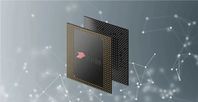
Huawei’s next flagship chip
Huawei is preparing to launch the Kirin 9050 together with the Mate 90 smartphone series this fall, and the Mate 90 line is expected in September 2026.
Pre-launch reporting around the processor says its overall performance exceeds Apple’s A18.
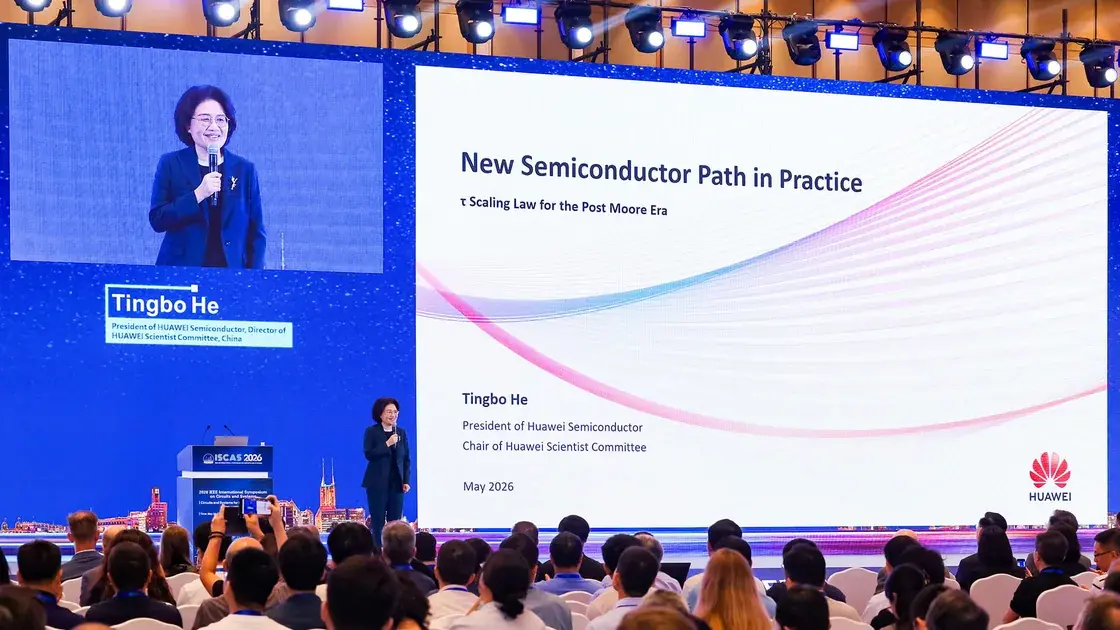
Those claims are linked to industry reporting as well as a presentation delivered at ISCAS 2026, the International Symposium on Circuits and Systems, held in Geneva.
The importance of the Kirin 9050 is tied not just to the performance comparison with Apple’s chip, but also to the method Huawei is using to get there.
The company’s upcoming flagship processor is described as reaching a level close to TSMC’s first-generation 3nm technology while avoiding dependence on the most advanced EUV lithography systems, which remain affected by export restrictions.
3D IC stacking as the core change
At the center of the design is a 3D IC stacking approach.
Instead of relying only on the standard progression toward smaller process nodes, this method raises transistor density by placing components in vertical layers.
That shift reduces the importance of traditional geometric scaling, which has long defined progress in semiconductor manufacturing.
In this case, the reported gain comes from architecture and integration.
By increasing density through vertical design, Huawei is said to improve performance without requiring the newest EUV tools.
That makes the Kirin 9050 notable as an example of an alternate engineering route rather than a direct replication of the conventional 3nm manufacturing path.
This approach is presented as a way to keep advancing performance under manufacturing constraints.
Rather than focusing solely on access to the smallest process technology, Huawei is described as using packaging and chip architecture to push its flagship processor closer to the performance class associated with much more advanced fabrication methods.
Tau Law and density gains
The theoretical basis for that strategy is Huawei’s proprietary Tau Law, developed by the company’s semiconductor research division.
Tau Law replaces conventional geometric miniaturization with what Huawei describes as temporal miniaturization.
In practical terms, the framework shifts the scaling problem away from feature-size reduction and toward better circuit timing and more efficient interconnect behavior.
Combined with 3D IC stacking, that approach is said to let Huawei work around EUV-related constraints through a different engineering method.
The claim is not simply that the company has matched an established process node by using the same route.
Instead, it is presented as achieving similar territory in density and performance through a different combination of design and manufacturing choices.
Huawei’s reported figures say transistor density on the Kirin 9050 is up 53.5% from the prior generation, reaching 238 million transistors per square millimeter.
That density is described as approaching the level of TSMC’s first-generation 3nm process technology while using manufacturing techniques that are more accessible.
The chip is also expected to deliver performance comparable to TSMC’s N31, a 3nm-class chip, while being built through a different manufacturing path based on legacy processes more widely available to Chinese semiconductor fabs.
What the Mate 90 launch may confirm
The Mate 90 series will be the first commercial test of these claims when it arrives this fall.
Huawei is positioning the next generation of flagship devices as part of a broader effort to rebuild its standing among leading smartphone vendors after several years of restrictions on access to advanced semiconductor manufacturing.
The main question for the launch is whether the reported specifications and conference-presented results hold up in production silicon.
If they do, Huawei would become the first Android smartphone maker to move ahead of Apple’s A-series chips in comprehensive benchmark performance, reversing a competitive gap that has lasted for years.
That puts the Kirin 9050 story in a broader context.
It is not only about one flagship processor, but about whether architecture, stacking, and interconnect optimization can sustain semiconductor progress when access to the newest lithography tools is limited.
Summary version for Medium
Huawei’s Kirin 9050 highlights 3D stacking and Tau Law ahead of the Mate 90 launch
Why this hardware shift matters for AI and compute buyers
Quick Summary: Huawei plans to introduce the Kirin 9050 with the Mate 90 series this fall, with September 2026 indicated for the phone launch window. Reports tied to industry channels and an ISCAS 2026 conference presentation describe the chip as moving past Apple’s A18 while nearing first-generation 3nm-class density.
Huawei’s next flagship chip
Huawei is preparing to launch the Kirin 9050 together with the Mate 90 smartphone series this fall, and the Mate 90 line is expected in September 2026. Pre-launch reporting around the processor says its overall performance exceeds Apple’s A18.
3D IC stacking as the core change
At the center of the design is a 3D IC stacking approach.
- Point 1: The central topic is chips-semiconductors, with the announcement framed around concrete operating detail.
- Point 2: Instead of relying only on the standard progression toward smaller process nodes, this method raises transistor density by placing components in vertical layers.
The useful takeaway is the operating constraint behind the announcement, not the announcement alone.
Tau Law and density gains
The theoretical basis for that strategy is Huawei’s proprietary Tau Law, developed by the company’s semiconductor research division. Tau Law replaces conventional geometric miniaturization with what Huawei describes as temporal miniaturization.
Read the Full Deep Dive
Want to explore the complete technical analysis, enterprise trade-offs, and detailed metrics?
Read the full article originally published at SendTech Times