Huawei's Tau scaling puts architecture at the center of China's AI-chip push
Huawei proposed Tau scaling, a framework focused on shorter signal paths rather than only smaller transistors. LogicFolding is planned for Kirin chips in fall and winter 2026, with Huawei claiming a density jump to 238 million transistors per square millimeter. The test is whether architecture-led gains can be validated in commercial chips amid export-control limits on advanced tools.
What happened
Huawei has introduced Tau scaling, a semiconductor development framework meant to improve chip performance as conventional transistor shrinking becomes harder.
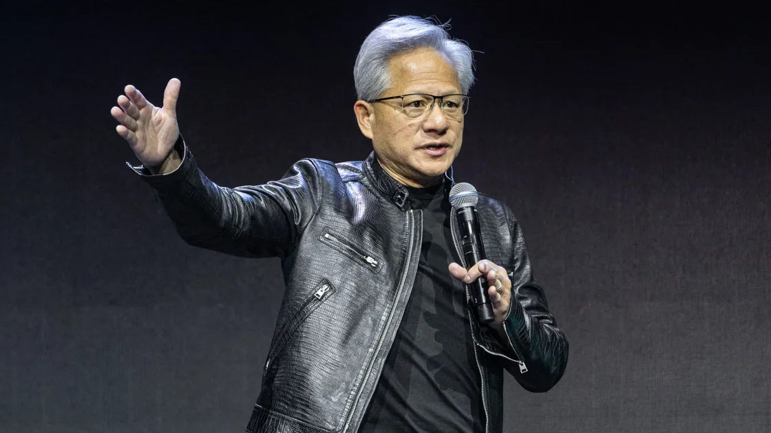
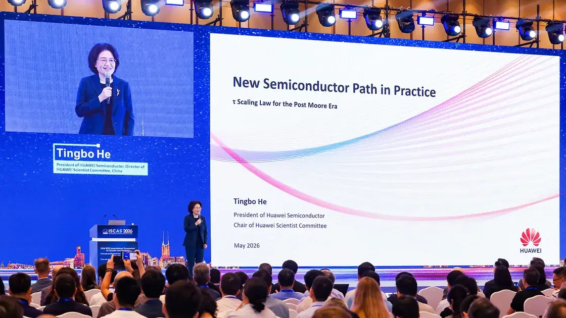
Huawei executive He Tingbo presented the proposal on May 25 at the IEEE International Symposium on Circuits and Systems in Shanghai.
KrASIA identifies He as the head of Huawei's semiconductor business and chair of the company's scientist committee.
The idea shifts emphasis from geometric scaling to time-based gains.
Rather than relying only on smaller transistors, Huawei is trying to shorten signal paths across devices, circuits, chips and systems.
Its LogicFolding architecture is the first practical step.
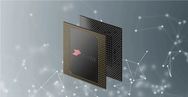
The company said Kirin chips planned for fall and winter 2026 will be the first to adopt the design.
Huawei said LogicFolding will move Kirin chips from a single-layer design to a double-layer structure.
He said density would rise from 155 million transistors per square millimeter to 238 million in 2026, after an earlier three-year move from 126 million to 155 million.
Why it matters
The market signal is not that Huawei has announced true 1.4-nanometer manufacturing.
KrASIA reports the goal as density comparable to 14 angstroms, or 1.4-nm-class processes, by 2031 through architecture, circuit design and system-level optimization.
That difference changes the story because Chinese chipmakers still face limits on advanced production tools under US and allied export controls.
If Huawei can validate performance gains through layout and signal-efficiency changes, it could ease some pressure on China's AI chip ecosystem.
It would not remove the need for commercial chips, manufacturing yields or independent benchmarks.
Who is affected
The immediate audience is China's AI chip sector, smartphone silicon teams and domestic semiconductor manufacturers trying to extend performance without matching the newest global nodes.
Customers watching future Kirin devices would also be affected if the claimed density gains translate into real products.
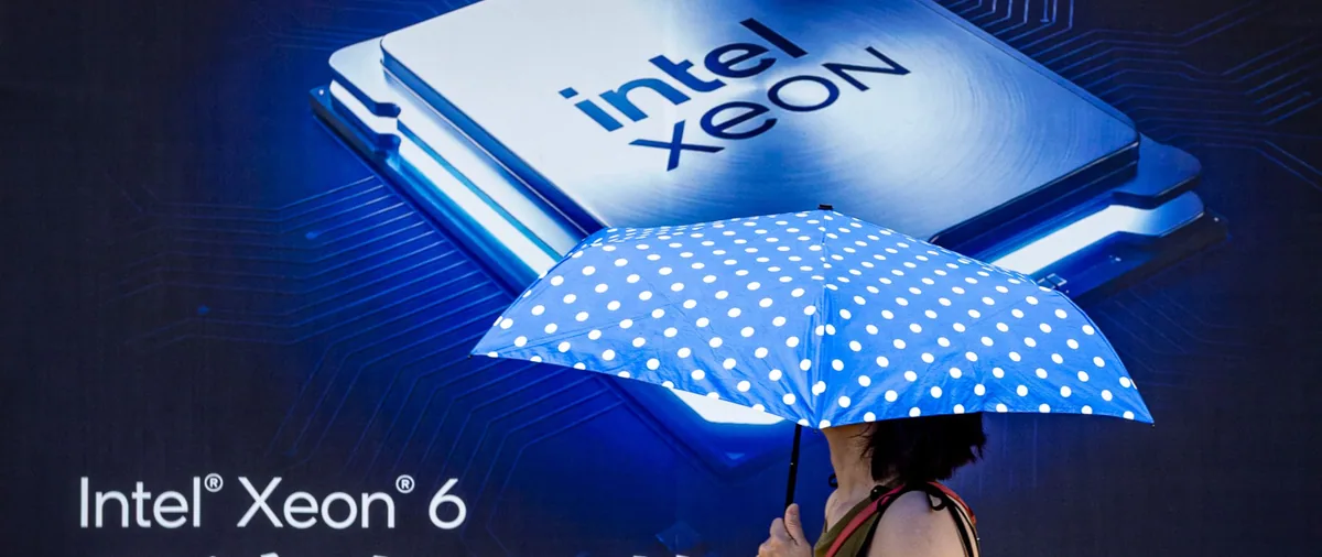
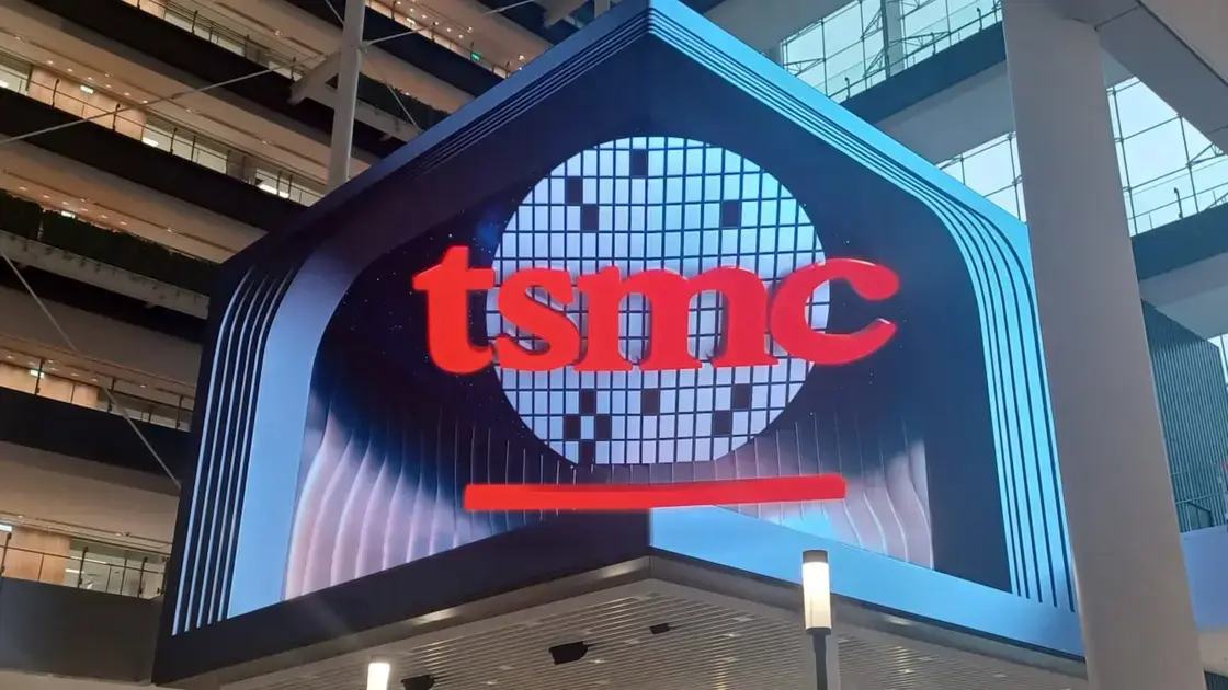
TSMC, Intel and Samsung remain the global comparison points.
TSMC announced its A14 1.4-nm-class process in 2025 and said production is planned for 2028, while Intel and Samsung are pursuing next-generation nodes around 2-nm and angstrom-class technologies.
What to watch next
The key test is whether LogicFolding appears in 2026 Kirin chips as described, and whether real-world performance, density and power results support Huawei's claims.
Readers should also watch whether Tau scaling becomes a repeatable roadmap or remains a one-generation architecture adjustment.
For AI infrastructure buyers, the practical question is whether the design can support competitive chips under real manufacturing constraints.
Summary version for Medium
Huawei's Tau scaling puts architecture at the center of China's AI-chip push
Why this hardware shift matters for AI and compute buyers
Quick Summary: Huawei proposed Tau scaling, a framework focused on shorter signal paths rather than only smaller transistors. LogicFolding is planned for Kirin chips in fall and winter 2026, with Huawei claiming a density jump to 238 million transistors per square millimeter.
What happened
Huawei has introduced Tau scaling, a semiconductor development framework meant to improve chip performance as conventional transistor shrinking becomes harder. Huawei executive He Tingbo presented the proposal on May 25 at the IEEE International Symposium on Circuits and Systems in Shanghai.
Why it matters
The market signal is not that Huawei has announced true 1.4-nanometer manufacturing.
- Point 1: The central topic is chips-semiconductors, with the announcement framed around concrete operating detail.
- Point 2: KrASIA reports the goal as density comparable to 14 angstroms, or 1.4-nm-class processes, by 2031 through architecture, circuit design and system-level optimization.
The important shift is not the AI label, but the operating boundary it creates for teams.
Who is affected
The immediate audience is China's AI chip sector, smartphone silicon teams and domestic semiconductor manufacturers trying to extend performance without matching the newest global nodes. Customers watching future Kirin devices would also be affected if the claimed density gains translate into real products.
Read the Full Deep Dive
Want to explore the complete technical analysis, enterprise trade-offs, and detailed metrics?
Read the full article originally published at SendTech Times