South Korea and Netherlands Expand Semiconductor Collaboration
The semiconductor partnership between South Korea and the Netherlands is evolving. New opportunities in silicon photonics are emerging as AI demands increase. This collaboration could reshape the future of chip technology and manufacturing.
EUR 1.1 billion is the investment aimed at enhancing silicon photonics capabilities.
On May 25, 2026, TrendForce reported that the semiconductor cooperation between South Korea and the Netherlands is set to advance beyond ASML's lithography technology.
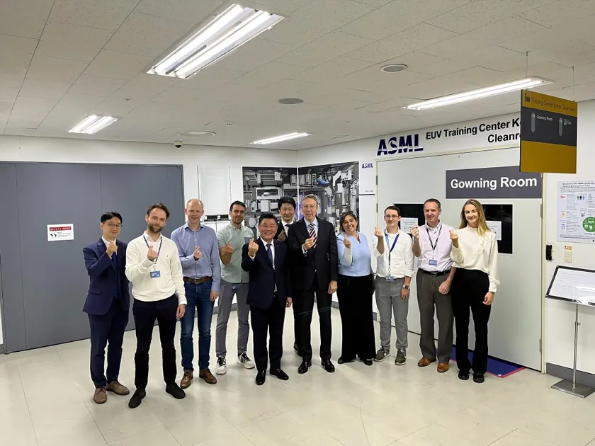
Dutch Ambassador Peter van der Vliet highlighted the potential for silicon photonics, a technology gaining traction as AI computing intensifies power demands in data centers.
Strengthening Optical Precision
The Netherlands is recognized for its optical precision, which is crucial for supporting silicon photonics development.
This technology is increasingly relevant as the semiconductor industry seeks to address the challenges posed by rising power consumption in advanced computing.
Investment in Silicon Photonics
PhotonDelta, a key Dutch photonics group, has secured a significant commitment of EUR 1.1 billion to establish a robust domestic silicon photonics ecosystem.
Wilbert Skap, PhotonDelta's investment manager, emphasized the importance of this initiative in fostering innovation in chip technology.
Samsung's Progress and Future Plans
In March, Samsung Electronics announced advancements in its silicon photonics foundry platform.
The company is also preparing to offer turnkey co-packaged optics services, expected to be available around 2029.
Broader Semiconductor Ties
The semiconductor relationship between South Korea and the Netherlands encompasses various Dutch equipment manufacturers beyond ASML.
ASM has strengthened its collaboration with South Korea by investing KRW 136.2 billion (approximately USD 91 million) to expand its atomic layer deposition equipment at the Hwaseong facility.
The Importance of Hybrid Bonding
BESI is becoming increasingly relevant as hybrid bonding equipment gains traction in advanced packaging.
Discussions around Samsung's adoption of this technology are anticipated to progress in the coming months.
Supply Chain Stability
To address concerns about supply chain vulnerabilities, South Korea and the Netherlands established a joint semiconductor supply-chain early warning system last year.
This initiative aims to mitigate risks associated with advanced chip equipment, materials, and packaging shortages.
Next Steps in Semiconductor Collaboration
As developments unfold, the semiconductor industry should monitor the outcomes of these collaborations, particularly the advancements in silicon photonics and hybrid bonding technologies.
The next significant milestone will be the anticipated rollout of Samsung's co-packaged optics services around 2029.
Summary version for Medium
South Korea and Netherlands Expand Semiconductor Collaboration
Why this hardware shift matters for AI and compute buyers
Quick Summary: The semiconductor partnership between South Korea and the Netherlands is evolving. New opportunities in silicon photonics are emerging as AI demands increase.
Strengthening Optical Precision
The Netherlands is recognized for its optical precision, which is crucial for supporting silicon photonics development. This technology is increasingly relevant as the semiconductor industry seeks to address the challenges posed by rising power consumption in advanced computing.
Investment in Silicon Photonics
PhotonDelta, a key Dutch photonics group, has secured a significant commitment of EUR 1.1 billion to establish a robust domestic silicon photonics ecosystem.
- Point 1: The central topic is semiconductors, with the announcement framed around concrete operating detail.
- Point 2: Wilbert Skap, PhotonDelta's investment manager, emphasized the importance of this initiative in fostering innovation in chip technology.
The important shift is not the AI label, but the operating boundary it creates for teams.
Samsung's Progress and Future Plans
In March, Samsung Electronics announced advancements in its silicon photonics foundry platform. The company is also preparing to offer turnkey co-packaged optics services, expected to be available around 2029.
Read the Full Deep Dive
Want to explore the complete technical analysis, enterprise trade-offs, and detailed metrics?
Read the full article originally published at SendTech Times