Intel Ships Panther Lake Chips Built With ASML High NA EUV
Intel has shipped selected Panther Lake processors made on Intel 18A with ASML High NA EUV lithography, Interesting Engineering reported, giving Intel production data while customer names, shipment volumes and wider node timing remain undisclosed.
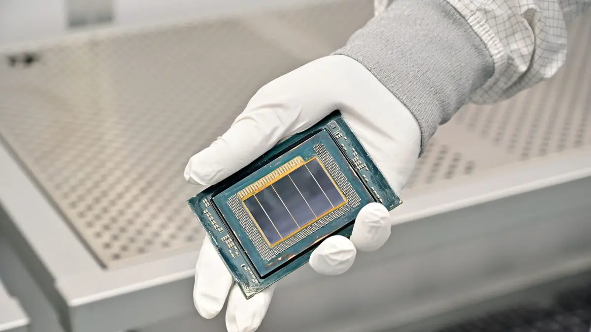
Selected Panther Lake processors are now shipping with ASML High NA EUV lithography in high-volume manufacturing, Interesting Engineering reported.
The commercial logic-product shipment covers a subset of Intel Core Ultra Series 3 processors made on the Intel 18A process.
Selected 18A layers are dual-qualified on ASML's platform at the Oregon site, with customer shipments matching yields on the existing NXE platform, the report said.
Panther Lake Uses Selected Lithography Layers
The newer exposure tool is being introduced on chosen layers rather than across the full chip stack.
Intel and ASML said the production run is being used to gather manufacturing data and refine system setup, uptime and implementation before broader use in future nodes.
The Panther Lake work keeps the existing production platform in the flow while adding the newer lithography step where the process can generate usable manufacturing evidence.
Interesting Engineering described the milestone as a move from research and early testing toward production manufacturing.
ASML Tooling Moves From Installation To Output
ASML's role follows a 2024 system placement at the Hillsboro, Oregon, research and development site, according to the report.
The chipmaker later installed and qualified ASML's second-generation TWINSCAN EXE:5200B system, which the report described as offering higher throughput, better overlay accuracy and an upgraded light source.
Christophe Fouquet, ASML's president and chief executive, said the technology brings increased resolution and better process control for smaller and denser chip patterning.
Naga Chandrasekaran, executive vice president and general manager of Intel Foundry, said the work shows how the newer EUV platform can be integrated into advanced semiconductor manufacturing at scale.
Wider Node Adoption Still Needs More Evidence
The milestone gives the foundry business production data for a lithography toolset expected to support denser chips and future AI-related computing demand.
The public material does not include customer names, shipment volume, wafer-output figures, cost impact, defect-rate comparisons or a dated schedule for using the toolset across additional process nodes.
For now, the source-backed development is narrower: selected 18A product layers are shipping in commercial high-volume logic products built with ASML's newer EUV platform.
The report does not include named customers, unit or wafer shipment volumes, comparative yield data, cost figures, defect-rate comparisons or a dated timeline for wider node adoption.
Summary version for Medium
Intel Ships Panther Lake Chips Built With ASML High NA EUV
Why this hardware shift matters for AI and compute buyers
Quick Summary: Intel has shipped selected Panther Lake processors made on Intel 18A with ASML High NA EUV lithography, Interesting Engineering reported, giving Intel production data while customer names, shipment volumes and wider node timing remain undisclosed.
Panther Lake Uses Selected Lithography Layers
The newer exposure tool is being introduced on chosen layers rather than across the full chip stack. Intel and ASML said the production run is being used to gather manufacturing data and refine system setup, uptime and implementation before broader use in future nodes.
ASML Tooling Moves From Installation To Output
ASML's role follows a 2024 system placement at the Hillsboro, Oregon, research and development site, according to the report.
- Point 1: The central topic is chips-semiconductors, with the announcement framed around concrete operating detail.
- Point 2: The chipmaker later installed and qualified ASML's second-generation TWINSCAN EXE:5200B system, which the report described as offering higher throughput, better overlay accuracy...
The important shift is not the AI label, but the operating boundary it creates for teams.
Wider Node Adoption Still Needs More Evidence
The milestone gives the foundry business production data for a lithography toolset expected to support denser chips and future AI-related computing demand. The public material does not include customer names, shipment volume, wafer-output figures, cost impact, defect-rate comparisons or a dated schedule for using the toolset across additional process nodes.
Read the Full Deep Dive
Want to explore the complete technical analysis, enterprise trade-offs, and detailed metrics?
Read the full article originally published at SendTech Times