Nvidia ‘likely the most concerned’ as Huawei bets on new chip architecture law
Huawei says its new Tau Scaling Law could support transistor density equivalent to a 1.4-nanometre process in high-end chips by 2031. Analysts said the move could weaken US-led export-control leverage as China pushes semiconductor self-sufficiency under sanctions. Omdia said Nvidia is likely the most concerned, while Chinese state media cast the effort as a technological Long March.
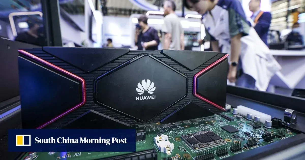
Huawei Technologies’ new chip architecture law is being read by analysts as a fresh test of whether China can push past US-led technology restrictions — and as a development that may worry Nvidia more than any other company.
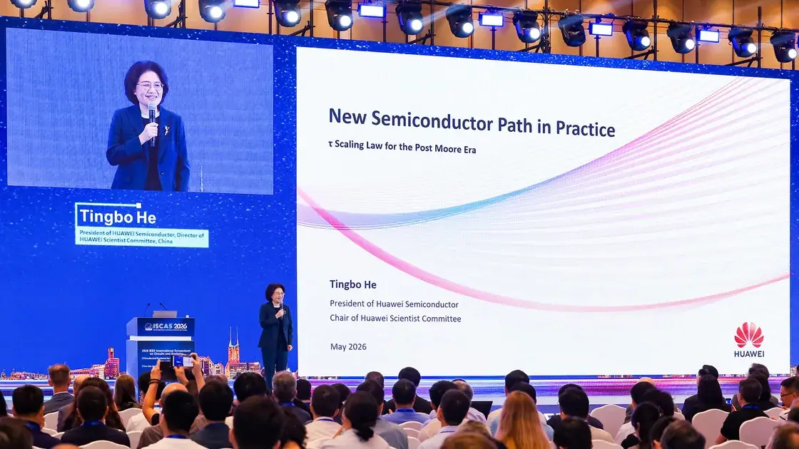
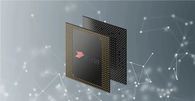
On Monday, Huawei introduced its Tau (τ) Scaling Law, which it said lays the groundwork to reach transistor density equivalent to a 1.4-nanometre process in high-end chips by 2031.
If that holds up in practice, it would narrow the gap with leading semiconductor companies and offer a new route around a manufacturing bottleneck created by sanctions.
Huawei’s case for a new path
Huawei said the new law could deliver performance gains in both smartphone chips and artificial intelligence computing systems.
US-led sanctions block China’s semiconductor industry from accessing the most advanced chipmaking technologies, including extreme ultraviolet lithography machines required for 3nm nodes and below.
He Tingbo, chairwoman of the Huawei Scientist Committee and president of Huawei’s semiconductor business department, said new EUV tools would no longer be necessary to reach these advanced nodes.
Liao Heng, chief scientist at Huawei’s semiconductor department, tied the approach to rising demand for computing power in the AI race.
“By 2035, our single chip module performance can be expected to increase by 100-fold, and system level performance can be expected to increase by 1,000 times,” Liao said.
He added that the path had “effectively tackled” the challenge of computing power availability, which he said was an anxiety in China and around the world.
Analysts link the move to export controls and Nvidia
Gary Ng, senior economist at Natixis Corporate and Investment Bank, said “the US will have less leverage over export control as China becomes more self-sufficient”, while cautioning that the Tau law still needed to be “tested in practice”.
James Lambert, head of Asia consulting at Oxford Economics, said the development pointed to China’s broader adaptation to Western technology restrictions.
He said Chinese firms were increasingly investing in alternative domestic AI and semiconductor pathways rather than depending on Western ones.
Wall Street research firm Bernstein called the announcement “another DeepSeek moment”.
Analyst Lin Qingyuan wrote that, if executed successfully, it could give the Chinese semiconductor industry more confidence to invest locally and build a fuller domestic semiconductor stack.
He Hui, director of semiconductor research at Omdia, said “Nvidia is likely the most concerned by this development”.
He said Nvidia had already lost half of its market share in China and now faced domestic chips that had nearly closed the gap with the H200.
The report also noted that China has yet to approve domestic sales of Nvidia’s H200 AI chips.
State media frames the effort as a Long March
Chinese state media welcomed the announcement in political terms.
Communist Party newspaper People’s Daily compared the struggle against US sanctions to “the most tragic and brave Long March in the history of science and technology”.
“Instead of getting stuck in a rut, why not try a different approach?” the paper wrote.
Summary version for Medium
Nvidia ‘likely the most concerned’ as Huawei bets on new chip architecture law
Why this hardware shift matters for AI and compute buyers
Quick Summary: Huawei says its new Tau Scaling Law could support transistor density equivalent to a 1.4-nanometre process in high-end chips by 2031. Analysts said the move could weaken US-led export-control leverage as China pushes semiconductor self-sufficiency under sanctions.
Huawei’s case for a new path
Huawei said the new law could deliver performance gains in both smartphone chips and artificial intelligence computing systems. US-led sanctions block China’s semiconductor industry from accessing the most advanced chipmaking technologies, including extreme ultraviolet lithography machines required for 3nm nodes and below.
Analysts link the move to export controls and Nvidia
Gary Ng, senior economist at Natixis Corporate and Investment Bank, said “the US will have less leverage over export control as China becomes more self-sufficient”, while cautioning that the Tau law still needed to be “tested in practice”.
- Point 1: The announcement adds a concrete operating detail that changes how buyers should read the story.
- Point 2: James Lambert, head of Asia consulting at Oxford Economics, said the development pointed to China’s broader adaptation to Western technology restrictions.
The important shift is not the AI label, but the operating boundary it creates for teams.
State media frames the effort as a Long March
Chinese state media welcomed the announcement in political terms. Communist Party newspaper People’s Daily compared the struggle against US sanctions to “the most tragic and brave Long March in the history of science and technology”.
Read the Full Deep Dive
Want to explore the complete technical analysis, enterprise trade-offs, and detailed metrics?
Read the full article originally published at SendTech Times