Huawei's Tau Law redefines chip scaling with logic folding as the post-Dennard path to 1.4nm
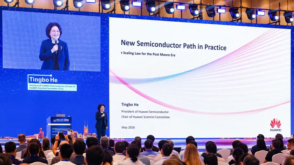
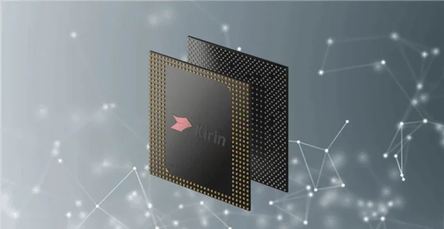
Huawei introduced the Tau Scaling Law at ISCAS 2026 in Shanghai as a semiconductor scaling framework built around temporal minimization through logic folding. The company said the approach could deliver transistor densities equivalent to 1.4nm by 2031, offering a path beyond geometric shrinking alone. Huawei also said it has already designed and shipped 381 chips using this architectural approach, with a new Kirin processor set to be the first commercial product with full logic folding technology.
Huawei used the 2026 International Symposium on Circuits and Systems in Shanghai to present the Tau Scaling Law, which the company described as a new semiconductor scaling framework centered on temporal minimization through logic folding.
He Tingbo, identified in the source as a Huawei Board Director and Semiconductor Division President, introduced the framework.
The source also said the Tau Scaling Law is referred to as “Her’s Law,” a name given by peers and colleagues.
A post-Dennard scaling framework
The source places Tau Law against the backdrop of Dennard scaling, which shaped semiconductor progress for decades by allowing smaller transistors to deliver more density, faster processors, and better power efficiency.
Huawei said that as transistors move toward atomic-scale dimensions, geometric shrinking by itself can no longer sustain the historical pace of improvement.
Tau Law is presented as a complementary path rather than a lithography-led one.
Instead of focusing only on making transistors smaller, the framework shifts attention to reducing the time needed for a signal to travel through and be processed by a chip.
How logic folding works
Huawei describes that timing-focused principle as temporal minimization.
Its practical mechanism is logic folding, a circuit reorganization technique intended to shorten computation pathways, compress signal routing, and extract more efficiency from each transistor.
this optimization spans the full stack, from device physics and circuit topology to system-level integration.
Huawei said that chips designed under Tau Law could reach transistor densities equivalent to 1.4nm process technology by 2031, reframing what a process node means as traditional geometric scaling plateaus.
Commercial proof point and industry implications
Huawei also argued that Tau Law is already in use rather than remaining a research concept.
The company said it has designed and shipped 381 chips using this architectural approach over the past six years.
It added that a new Kirin smartphone processor launching this fall will incorporate full logic folding technology, making it the first commercial proof point for the framework.
The source said Tau Law matters to the global semiconductor industry because it offers a scaling path that does not depend exclusively on advances in EUV lithography.
Those advances, the source noted, are becoming more expensive and are politically restricted for non-Western manufacturers.
In that framing, logic folding is positioned as a system-level answer to a device-level problem, with its commercial results likely to be watched closely by chip designers.
Summary version for Medium
Huawei's Tau Law redefines chip scaling with logic folding as the post-Dennard path to 1.4nm
Why this hardware shift matters for AI and compute buyers
Quick Summary: Huawei introduced the Tau Scaling Law at ISCAS 2026 in Shanghai as a semiconductor scaling framework built around temporal minimization through logic folding. The company said the approach could deliver transistor densities equivalent to 1.4nm by 2031, offering a path beyond geometric shrinking alone.
A post-Dennard scaling framework
The source places Tau Law against the backdrop of Dennard scaling, which shaped semiconductor progress for decades by allowing smaller transistors to deliver more density, faster processors, and better power efficiency. Huawei said that as transistors move toward atomic-scale dimensions, geometric shrinking by itself can no longer sustain the historical pace of improvement.
How logic folding works
Huawei describes that timing-focused principle as temporal minimization.
- Point 1: The central topic is science-tech, with the announcement framed around concrete operating detail.
- Point 2: Its practical mechanism is logic folding, a circuit reorganization technique intended to shorten computation pathways, compress signal routing, and extract more efficiency from...
The useful takeaway is the operating constraint behind the announcement, not the announcement alone.
Commercial proof point and industry implications
Huawei also argued that Tau Law is already in use rather than remaining a research concept. The company said it has designed and shipped 381 chips using this architectural approach over the past six years.
Read the Full Deep Dive
Want to explore the complete technical analysis, enterprise trade-offs, and detailed metrics?
Read the full article originally published at SendTech Times