Samsung Samples 12-Layer HBM4E for Next-Generation AI Accelerators
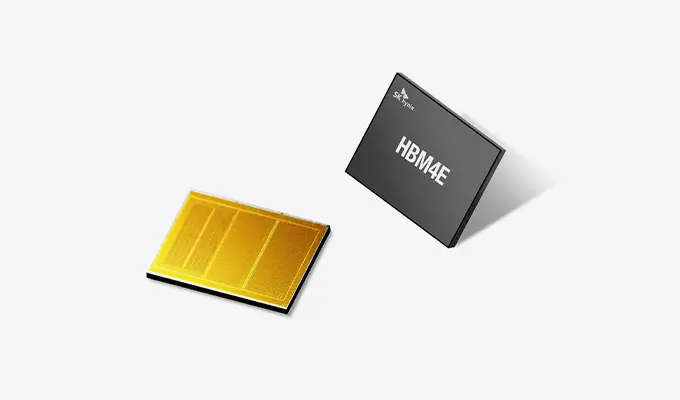
Samsung has shipped samples of a 12-layer HBM4E memory product for next-generation AI accelerators. The reported specifications include up to 16Gbps per pin, 3.6TB/s per stack and a 48GB 12-layer configuration. The company says improved efficiency and thermal characteristics are intended to support AI data-center workloads.
Samsung Pushes HBM4E Into the AI Memory Race
Samsung Electronics has begun shipping samples of what it describes as the world's first 12-layer HBM4E memory to global customers, a move aimed at strengthening its position in the high-bandwidth memory market for advanced AI accelerators.
The Korean company said the new product is designed for the next generation of AI systems, where model training and inference workloads require faster memory bandwidth, higher stack capacity and better power efficiency.
The sample shipment follows Samsung's earlier HBM4 mass-production milestone and signals that the company is trying to move quickly into the next performance tier.
Performance and Capacity Targets
Samsung's 12-layer HBM4E supports stable operation at 14Gbps per pin and can reach up to 16Gbps.
The company also cites bandwidth of 3.6TB per second from a single stack, a specification intended to support large language models and other high-throughput AI computing systems.
The product offers 48GB of capacity in the 12-layer configuration, more than the previous generation .
Samsung also plans to widen the line-up for different customer environments, including 32GB eight-layer and 64GB sixteen-layer versions.
For AI infrastructure operators, the practical importance is not only peak speed.
Denser and faster memory can reduce bottlenecks around accelerators, especially as frontier models and inference services place heavier pressure on data movement between compute and memory.
Process, Packaging and Efficiency
Samsung's HBM4E combines 1c DRAM, described as a sixth-generation 10-nanometer-class process, with a 4-nanometer logic die from the company's foundry operations.
The report frames this as part of Samsung's broader turnkey advantage across memory, foundry, system LSI and advanced packaging.
The company also claims a 16% improvement in energy efficiency and more than a 14% improvement in thermal resistance compared with HBM4.
Those efficiency and heat-management gains matter because AI data centers are increasingly constrained by power consumption and cooling as much as by raw chip supply.
What Comes Next
Samsung plans to move from samples to mass supply according to customer schedules.
Hwang Sang-joon, vice president in Samsung's memory business, said the HBM4E sampling reinforces the company's technology leadership after its HBM4 production progress and that Samsung will continue investing in production infrastructure for the AI memory market.
The announcement also raises competitive pressure in HBM, a segment where memory suppliers are racing to secure design wins with AI accelerator makers and hyperscale cloud customers.
If Samsung can convert the new samples into validated volume shipments, HBM4E could become a key part of its effort to regain momentum in premium AI memory.
Summary version for Medium
Samsung Samples 12-Layer HBM4E for Next-Generation AI Accelerators
Why Samsung Samples 12-Layer HBM4E matter now for cloud infrastructure teams
Quick Summary: Samsung has shipped samples of a 12-layer HBM4E memory product for next-generation AI accelerators. The reported specifications include up to 16Gbps per pin, 3.6TB/s per stack and a 48GB 12-layer configuration.
Samsung Pushes HBM4E Into the AI Memory Race
Samsung Electronics has begun shipping samples of what it describes as the world's first 12-layer HBM4E memory to global customers, a move aimed at strengthening its position in the high-bandwidth memory market for advanced AI accelerators. The Korean company said the new product is designed for the next generation of AI systems, where model training and inference workloads require faster memory bandwidth, higher stack capacity and better power efficiency.
Performance and Capacity Targets
According to the source report, Samsung's 12-layer HBM4E supports stable operation at 14Gbps per pin and can reach up to 16Gbps.
- Point 1: The central topic is cloud-data-centers, with the announcement framed around concrete operating detail.
- Point 2: The company also cites bandwidth of 3.6TB per second from a single stack, a specification intended to support large language models and other high-throughput AI computing systems.
The important shift is not the AI label, but the operating boundary it creates for teams.
Process, Packaging and Efficiency
Samsung's HBM4E combines 1c DRAM, described as a sixth-generation 10-nanometer-class process, with a 4-nanometer logic die from the company's foundry operations. The report frames this as part of Samsung's broader turnkey advantage across memory, foundry, system LSI and advanced packaging.
Read the Full Deep Dive
Want to explore the complete technical analysis, enterprise trade-offs, and detailed metrics?
Read the full article originally published at SendTech Times