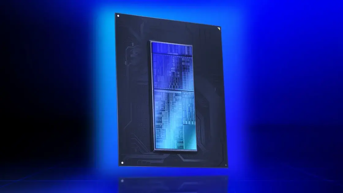
SK hynix Memristor AI Chip Shows 21.3 TOPS/W But Leaves Throughput Gap
SK hynix, TetraMem and USC researchers developed a 65 nm memristor-based in-memory computing chip for edge AI. The paper listed 21.3 TOPS/W at 100 MHz, but the demonstration left four of 10 NPUs idle and did not disclose full-chip saturated throughput.

SK hynix, TetraMem and University of Southern California researchers have built a memristor-based in-memory computing chip for edge AI, but the strongest disclosed result is efficiency rather than proven full-chip throughput.
The SK hynix TetraMem memristor AI chip targets lightweight neural-network inference by moving analogue computation into memory arrays.
The paper describes a 10-NPU design, while leaving simultaneous saturation and sustained full-chip throughput outside the disclosed benchmark.
SK hynix And TetraMem Built A 65 nm Edge AI Test Chip
The researchers developed a system-on-chip for edge AI devices using memristor-based in-memory computing.
The chip is designed to accelerate lightweight neural networks by reducing data movement between memory and compute logic, a constraint for small devices with limited power and heat budgets.
The reported design uses an embedded RISC-V processor to schedule work across 10 neural processing units.
One of those NPUs is dedicated to depthwise convolution, while the other nine handle pointwise and dense operations.
The paper says SK hynix fabricated the memristor devices and integrated the resistive switching cells above 65 nm CMOS circuitry using its back-end process.
The 65 nm fabrication evidence keeps the result in research-stage territory: the disclosed work is a proof-of-concept, not a commercial edge AI processor with a launch plan.
Depthwise Convolution Gets A Dedicated NPU
Depthwise convolution is common in lightweight models such as MobileNet, but the paper describes weak mapping onto conventional crossbar arrays because each channel is filtered separately and has limited data reuse.
The research team built a separate NPU for that workload rather than relying only on standard in-memory compute blocks.
According to the paper, each of the nine standard NPUs includes a 256 × 256 memristor crossbar for analogue vector-matrix multiplication, 256 8-bit digital-to-analogue converters, 256 8-bit analogue-to-digital converters and additional peripheral circuitry.
According to the paper, the dedicated depthwise-convolution NPU instead uses eight 252 × 28 zig-zag crossbar blocks.
According to the paper, those diagonal selection lines activate 252 memory cells across 28 columns.
The paper says the design allows 28 independent 3 × 3 convolutions to run in parallel while using all of the array for weight storage.
MobileNet Test Shows Efficiency, Not Full-Chip Throughput
The research team demonstrated the chip with a customised MobileNetV1Small network on the Visual Wake Words benchmark.
According to the paper, the network contained about 36,000 parameters, with depthwise layers assigned to the dedicated NPU and pointwise layers assigned to standard NPUs.
The hardware executes unsigned analogue vector-matrix multiplication, so the research setup converted inputs and weights to unsigned 8-bit values before execution.
Memristor programming accuracy was only slightly above 2 bits, and the design used a two-subarray compensation technique to reach roughly 4 bits of effective weight precision.
The paper described 80.36% end-to-end inference accuracy, matching the corresponding 4-bit software model.
It also listed 0.254 TOPS peak throughput per NPU.
At 100 MHz, the paper gave energy efficiency of 21.3 TOPS/W; at 400 MHz, it gave 11.9 TOPS/W.
The efficiency figures are specific, but the performance baseline remains narrow.
The demonstration used one dedicated depthwise-convolution NPU and five standard NPUs, leaving four standard NPUs idle.
The 2.54 TOPS Figure Remains Theoretical
The reported full-chip peak reaches about 2.54 TOPS only by extending the per-NPU figure across all 10 NPUs.
That total remains theoretical because the paper does not show sustained throughput for a real network using every NPU at once.
The same limitation affects comparisons with larger AI processors.
The paper claims the chip exceeds Nvidia A100 INT8 energy efficiency by an order of magnitude, but the public evidence does not include an independently substantiated complete full-chip workload result.
Edge AI hardware still needs usable throughput, stable accuracy and production-ready software support alongside low power draw.
The current evidence shows a fabricated research chip and a benchmark demonstration, not a validated commercial platform.
SK hynix, TetraMem and USC did not disclose full SoC throughput under simultaneous 10-NPU saturation, sustained real-network throughput, commercial availability, software tooling, customer validation or a production process roadmap for the memristor chip.
Summary version for Medium
SK hynix Memristor AI Chip Shows 21.3 TOPS/W But Leaves Throughput Gap
Why this hardware shift matters for AI and compute buyers
Quick Summary: SK hynix, TetraMem and USC researchers developed a 65 nm memristor-based in-memory computing chip for edge AI. The paper listed 21.3 TOPS/W at 100 MHz, but the demonstration left four of 10 NPUs idle and did not disclose full-chip saturated throughput.
SK hynix And TetraMem Built A 65 nm Edge AI Test Chip
The researchers developed a system-on-chip for edge AI devices using memristor-based in-memory computing. The chip is designed to accelerate lightweight neural networks by reducing data movement between memory and compute logic, a constraint for small devices with limited power and heat budgets.
Depthwise Convolution Gets A Dedicated NPU
Depthwise convolution is common in lightweight models such as MobileNet, but the paper describes weak mapping onto conventional crossbar arrays because each channel is filtered separately and has limited data reuse.
- Point 1: The central topic is chips-semiconductors, with the announcement framed around concrete operating detail.
- Point 2: The research team built a separate NPU for that workload rather than relying only on standard in-memory compute blocks.
The important shift is not the AI label, but the operating boundary it creates for teams.
MobileNet Test Shows Efficiency, Not Full-Chip Throughput
The research team demonstrated the chip with a customised MobileNetV1Small network on the Visual Wake Words benchmark. According to the paper, the network contained about 36,000 parameters, with depthwise layers assigned to the dedicated NPU and pointwise layers assigned to standard NPUs.
Read the Full Deep Dive
Want to explore the complete technical analysis, enterprise trade-offs, and detailed metrics?
Read the full article originally published at SendTech Times