Imec Says AI Inference Pushes Optical I/O Closer To Chips
Imec researchers told EE Times that AI inference is shifting the interconnect problem from rack-scale optics towards 2.5D and 3D optical I/O near processors. The group discussed a 250 Tb/s bandwidth projection but did not disclose commercial product timing, customer deployments or cooling test results.
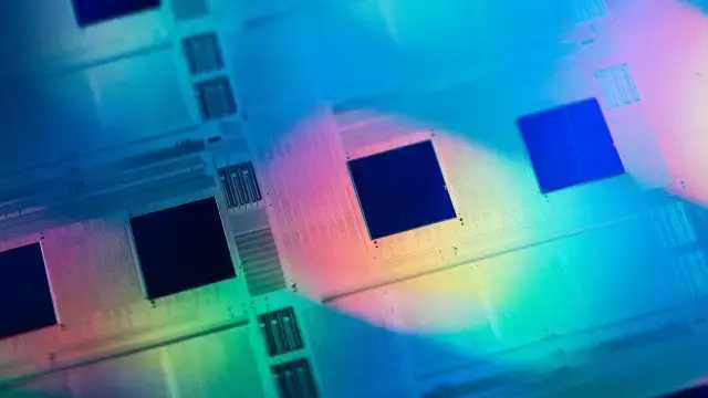
Imec researchers say AI inference is pushing the optical I/O roadmap closer to processors, because large models now need faster movement of data between accelerators as well as more compute.
The AI inference optical I/O roadmap described by imec starts with co-packaged optics, but the research group says future systems may need 2.5D and 3D integration to control bandwidth, latency and power.
Imec Projects 250 Tb/s Bandwidth Demand For Future AI Processors
Peter Ossieur, portfolio director at imec and professor at Ghent University, told EE Times that inference needs to be reactive because it is the moment when users interact with a model.
EE Times said those workloads can combine extended prompts, retrieval tools, reasoning chains, multimodal inputs and agent-style systems.
EE Times described scale-up networking as the more difficult domain.
Scale-out networks connect racks and systems across a data centre, while scale-up links GPUs or other accelerators tightly enough that applications can treat them as one larger processor.
EE Times said today's scale-up fabric is often copper-based and mostly constrained to the rack.
It said that model becomes harder as AI systems move towards hundreds, thousands or tens of thousands of accelerators working together.
Co-Packaged Optics Is Not The End Of Imec's Roadmap
Imene Jadli, portfolio manager for optical interconnect at imec, told EE Times that co-packaged optics is a logical next step but not the end of the roadmap.
Co-packaged optics moves optical engines into the package and shortens the electrical path between the optical module and the processor or switch.
The power limit is the main constraint in the figures discussed by imec.
EE Times said one future-system projection used by imec puts processor input and output bandwidth at roughly 250 Tb/s.
It said anticipated co-packaged optics approaches could require about 1.25 kW for the optics alone, on top of processors that may already consume several kilowatts.
Ossieur told EE Times that imec needs an approach that is better than co-packaged optics.
The research group's proposed path is 2.5D optical I/O, where optics is integrated at the interposer or substrate level to shorten the electrical path and lower the power needed to move data.
2.5D Optical I/O Could Cut Optical Power Below 200 W
Ossieur said the same imec projection showed 2.5D optical I/O reducing optical power from about 1.25 kW to below 200 W.
EE Times said imec describes the approach as "wide and slow", using many lanes at moderate speeds instead of a smaller number of very high-speed lanes with heavier signal processing.
The materials work remains broad.
EE Times said co-packaged optics still needs compact, efficient and high-bandwidth devices, including electro-absorption modulators and high-speed photodetectors.
It said imec is exploring barium titanate and III-V compounds alongside silicon photonics because silicon remains attractive for CMOS manufacturing but may not provide every property needed for future optical I/O.
Imec's longer-term endpoint is 3D optical I/O, where optics becomes part of the 3D compute stack.
EE Times said that roadmap could move optical links into advanced packages for processor-to-processor and memory-to-processor data movement, including high-bandwidth memory and stacked processors.
Imec did not disclose a commercial product timetable, named AI-system customers, manufacturing-yield data, optical-coupling results or cooling test results for 3D optical I/O.
Summary version for Medium
Imec Says AI Inference Pushes Optical I/O Closer To Chips
Why this hardware shift matters for AI and compute buyers
Quick Summary: Imec researchers told EE Times that AI inference is shifting the interconnect problem from rack-scale optics towards 2.5D and 3D optical I/O near processors. The group discussed a 250 Tb/s bandwidth projection but did not disclose commercial product timing, customer deployments or cooling test results.
Imec Projects 250 Tb/s Bandwidth Demand For Future AI Processors
Peter Ossieur, portfolio director at imec and professor at Ghent University, told EE Times that inference needs to be reactive because it is the moment when users interact with a model. EE Times said those workloads can combine extended prompts, retrieval tools, reasoning chains, multimodal inputs and agent-style systems.
Co-Packaged Optics Is Not The End Of Imec's Roadmap
Imene Jadli, portfolio manager for optical interconnect at imec, told EE Times that co-packaged optics is a logical next step but not the end of the roadmap.
- Point 1: The central topic is chips-semiconductors, with the announcement framed around concrete operating detail.
- Point 2: Co-packaged optics moves optical engines into the package and shortens the electrical path between the optical module and the processor or switch.
The important shift is not the AI label, but the operating boundary it creates for teams.
2.5D Optical I/O Could Cut Optical Power Below 200 W
Ossieur said the same imec projection showed 2.5D optical I/O reducing optical power from about 1.25 kW to below 200 W. EE Times said imec describes the approach as "wide and slow", using many lanes at moderate speeds instead of a smaller number of very high-speed lanes with heavier signal processing.
Read the Full Deep Dive
Want to explore the complete technical analysis, enterprise trade-offs, and detailed metrics?
Read the full article originally published at SendTech Times